Popular searches
-
Products
-
Hyaluronic Acid
-
Medical Grade Sodium Hyaluronate
High-purity medical-grade, used in ophthalmic surgery and eye drops
Cosmetic Grade Sodium Hyaluronate
Hydrating, plumping, smoothing, and film-forming
Food Grade Hyaluronic Acid
Oral supplement to support joint comfort and skin hydration
Injection Grade Sodium Hyaluronate
Cross-linked HA for joint lubrication and dermal fillers
Micro Hyaluronic Acid
Super active hyaluronic acid, Molecular weight: <5k Da
Hyaluronic Acid Elastomer
A long-lasting, sculpting filler for enhanced support and shape
-
-
Pharmaceuticals
-
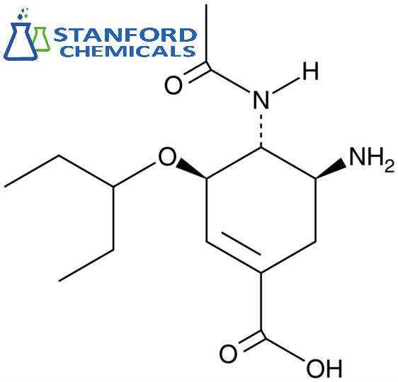
Remdesivir
Inhibits viral replication for treating COVID-19
3-Amino-2-chloro-4-methylpyridine
Chlorinated amino-methyl derivative of a pyridine base
4-Bromopyrazole
Bromo-substituted, five-membered nitrogen heterocycle
Folic Acid
For anemia or pregnancy supplementation
Chondroitin Sulfate
A dietary supplement or adjunct therapy for osteoarthritis
Vitamin B3
For pellagra or metabolic support
-
-
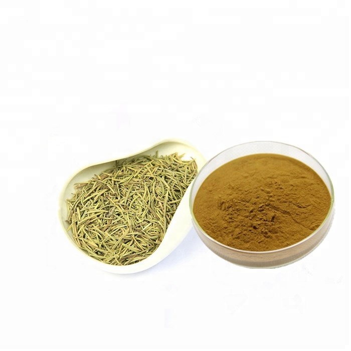
Herbal Extract
-
Apigenin
Antioxidant, antiviral, anti-inflammatory, calming and tranquilizing
Fisetin
Potent antioxidant activity, with potential to delay aging
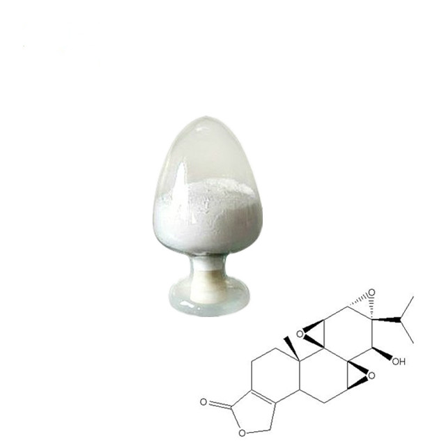
Artemisinin
Antimalarial, antitumor, immune-modulating
Dihydromyricetin
Supports liver health and metabolic function
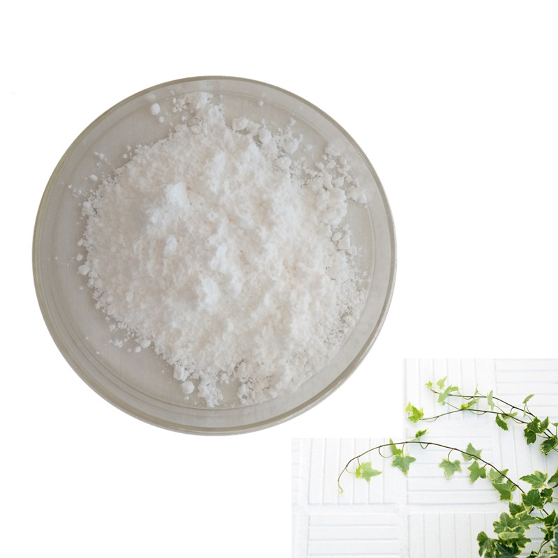
Salicin
Natural precursor to aspirin, relieves pain
CoenzymeQ10
Provides power to the heart, muscles, and other organs.
-
-
Applications
-
About Us